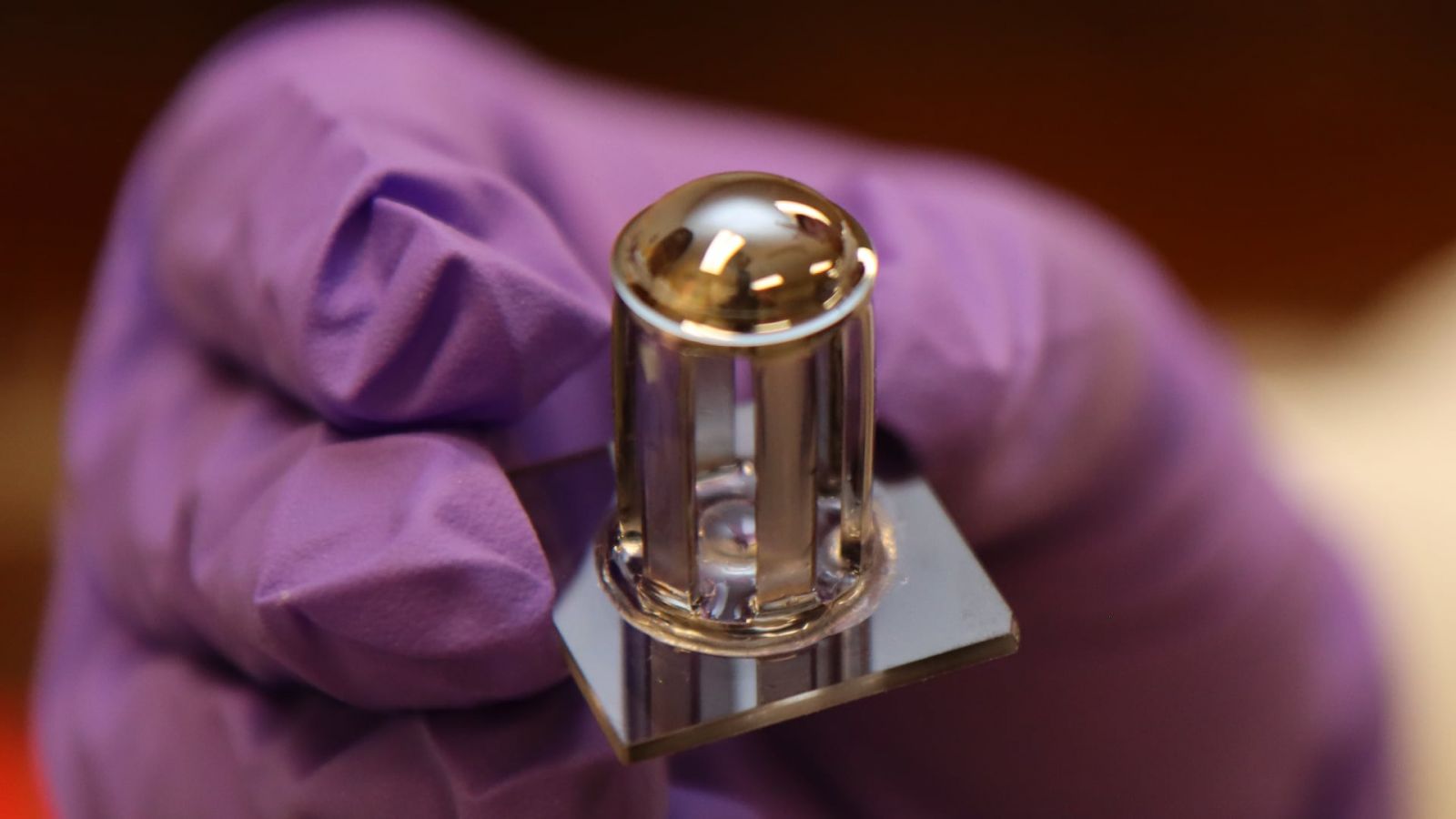
Huachao Mao, assistant professor of engineering technology in Purdue University’s Polytechnic college, and his team have created a method to fabricate economical multilevel microfluidic devices as small 10 microns deep and 100 microns wide. The patent-pending innovation could be useful to researchers in biomedical, environmental testing, geology, manufacturing and other fields.
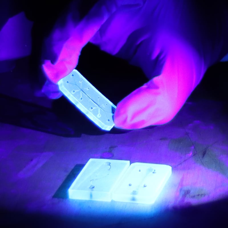 One micron is one-millionth of a meter; 10 microns are one-tenth of the diameter of a human hair. Microfluidic devices are diagnostic systems that analyze small volumes of materials rapidly and accurately.
Applications for the new method include cancer cell analysis, drug screenings, environmental testing, geology, manufacturing, single-cell isolation and point-of-care diagnostics.
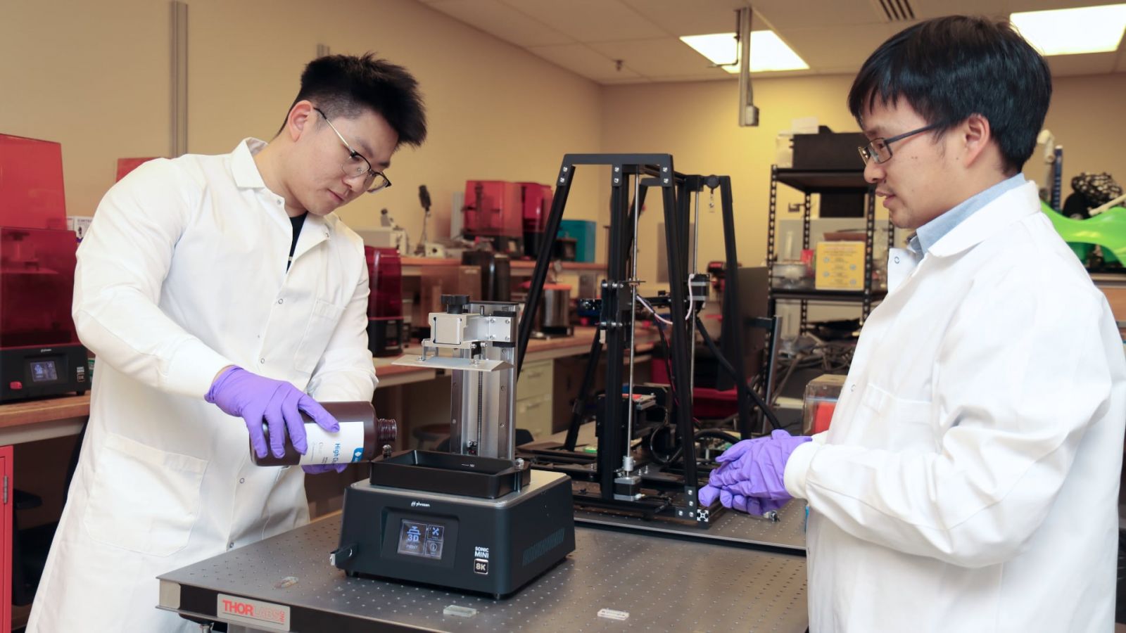
Vat photopolymerization (VPP) improves upon traditional fabrication methods and 3D printing, according to Mao.
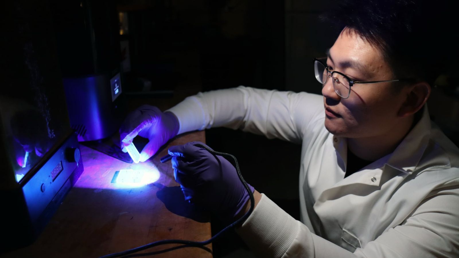
“VPP allows for the direct fabrication of highly transparent microfluidics with a much higher resolution, allowing for channels as narrow as 100 microns,” said Mao. “An emerging method within VPP is the use of liquid crystal display (LCD) technology, which uses ultraviolet light to facilitate the photopolymer solidification process.”
Biomedical research can be accelerated by precisely controlling fluid flow and reaction conditions at the microliter or nanoliter scale. These devices also improve the accuracy and speed of diagnostic tests and enable portable testing solutions across diverse fields.
“The traditional method to fabricate microfluidic devices is costly and time-consuming,” Mao said. “Fabrication takes several steps and requires high-end equipment and a cleanroom environment.”
Mao and his team conduct research in Purdue Polytechnic’s Additive and Intelligent Manufacturing Lab.
See the full story by Purdue Research Foundation’s Steve Martin.